Recently, Enterprise Storage Forum published an article by Henry Newman in which he argued that lithography limits and disk drive density are going to keep solid state disks (SSDs) from replacing spinning disks. To help explain his argument, I’m going to outline why one of the keys to this equation, SSD density, is in grave […]
Recently, Enterprise Storage Forum published an article by Henry Newman in which he argued that lithography limits and disk drive density are going to keep solid state disks (SSDs) from replacing spinning disks. To help explain his argument, I’m going to outline why one of the keys to this equation, SSD density, is in grave danger of stopping next year.
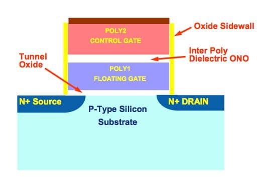
The SSDs that we’re using today are built on floating gate transistor technology, illustrated in Figure 1 below from Anandtech.

To program (write) to the transistor, which creates a logical 0, a positive voltage is applied to the drain which activates the electrons underneath the floating gate in the substrate. Then a larger positive voltage is applied to the control gate forcing the electrons to tunnel into the floating gate.
To erase the transistor, or to remove the extra electrons, a negative voltage is applied to the control gate and a positive voltage is applied to the source. This forces the electrons out of the floating gate and into the source.
To read the transistor, a positive voltage that is much lower than the write voltage is applied to the control gate. An additional positive voltage, also lower than the write voltage, is applied to the drain. The current between the source and the drain will determine if the floating gate has extra electrons (logical 0) or does not (logical 1).
This is the basic concept transistors use to store data in the SSD. Constructing SSDs from NAND is a bit more challenging and something like assembling a pyramid of pachyderms.
With NAND Flash, the floating-gate transistor is used as the basis for SSDs. The first step is to daisy-chain the transistors (gates) in series. Typically 32 gates are chained in series. These groups are connected in a NOR style where each line is connected directly to ground and the other is connected to a bit line. This arrangement has advantages for cost, density, and power as well as performance but it is a compromise that has some implications.
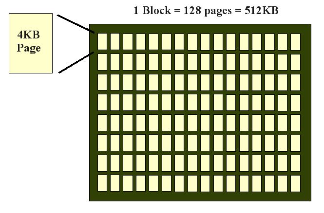
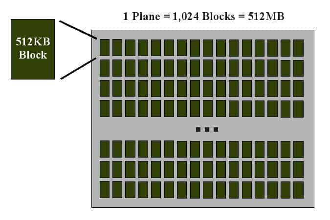
A number of these groups are then combined into pages (or sub-pages). The typical page is 4KB in size. The pages are then combined to form a block. A block, illustrated below in Figure 2, is typically formed from 128 pages giving a block a size of 512KB.


Constructing drives is fairly straightforward is not dissimilar to creating memory DIMMs. But there are a number of issues that need to be addressed for SSDs to be successful and, perhaps more importantly, these issues are particularly sensitive to the lithography size.
One of the coolest things about SSDs is that they don’t contain spinning media, which greatly reduces latencies and increases potential throughput. Reading, writing, and erasing are all done electrically as opposed to spinning media, where a large part of the latency is due to mechanical movement of the read/write heads and waiting for the particular block to spin around to the right spot. With SSDs, voltages are applied to the chips to cause an I/O operation . However, everything is not as easy as it seems.
Recall that the transistors are connected in series. To measure the state of any particular cell, all cells in the series have to be in a conductive state. This is accomplished by applying a bias voltage of +5V that is high enough to turn on all the gates in the series so that the particular cell that has the desired data can be read reliably enough, or written to (programmed), or erased.
The details of the read process are a bit involved and beyond the scope of this article, but it begins by applying the +5V bias voltage. Then a 0.5V voltage is applied above the bias voltage to read a particular cell. Notice that the bias voltage is a factor of 10 greater than the voltage needed to read the cell.
Writing to the cells is similar to reading, but the voltages are much higher. For writing or erasing to cells the voltages can be as high as 20V.
An important observation is that to read, write, or program a particular cell, the +5V bias voltage has to be applied. This is much larger than the read voltage of 0.5V but not as large as the program voltage (20V). Even more important is that the bias voltage is applied to all cells in the line (series) even if only one cell in the series is to be used. For example, to read one cell, a voltage 10 times greater than the actual read voltage has to be applied to all gates in the line. Moreover, typically there is never just a single line that is being read so almost all cells in the block are subjected to the +5V bias voltage. Over time, the electromagnetic (EM) field created by the bias voltage affects all cells, ultimately impacting the voltage level needed to program or write to the cell. In fact, it reduces the voltage level required to program the cell.
For a brand spanking new cell, the voltage required for programming is around 20V so that you can write to the cell or erase the data. But, over time, applying all the various voltages necessary for an I/O operation will impact the voltage required to program the cell.
Since not every cell has the same voltage applied at the same time, each cell will have its own individual required programming voltage. However, to accommodate the worst case, a programming voltage of 20V is applied every time. This can be bad for erasing data because the erase has to happen on a block level so all cells have to be subjected to the same voltage level (20V). This can cause the cells to actually push out more electrons than required for erasing. This phenomenon is sometimes referred to as “deep-erasing.” If a cell is deep-erased then the next time it is programmed it may not have enough electrons to be measured correctly. This is compensated by a “verify” step of the write cycle that detects the problem and repeats the write cycle until the cell achieves the correct charge (number of electrons). But, having to do this reduces the performance of the SSD because it is just this one cell that does not have the correct number of electrons. Good SSD controllers can recognize this problem and deactivate the particular line on the page or deactivate the page and use a page from the “pool” of backup pages. There has even been discussion of using a lower program voltage as the block ages.
One can see that there are many aspects to making SSDs work correctly and repeatedly. One thing to remember is that without changes to the materials or the techniques for storing and retrieving data, the voltages and associated problems stay the same.
Potential SSD issues go beyond deep-erase problems. As a result of the voltages being applied to the cells, EM fields are created within the SSD. While designers have gone to great lengths to isolate cells from one another, the fields from one cell can extend to another. The effects of a field from a neighboring cell or line may have some impact on a particular cell. A fresh SSD will have cells that need approximately +5V for the bias voltage, 0.5V for a read voltage, and 20V for programming/erasing. But over time, the required voltage for programming a cell actually decreases. During programming, a cell will create a field large enough to perhaps change the properties of a neighboring cell. While designers go to great lengths to make sure that this doesn’t happen or that the SSD can compensate for this happening, this phenomenon still occurs and can lead to silent data corruption.
The silent data corruption scenario is fairly simple – a cell has some voltage applied to it, a bias voltage or a program/erase voltage. The resulting field can disturb neighboring cells changing their properties. For example, the number of electrons in the cell can decrease or electrons can be tunneled into the cell. In either case, it’s possible to change the value in the cell silently.
Designers are aware of this issue and have created techniques to prevent data corruption. However, these techniques cost money and no one wants to make SSDs more expensive. As a result, most SSDs are designed to meet JEDEC’s data retention requirements meaning that a brand new SSD should be able to store data at least 10 years (when the SSD has more write/erase usage, the data retention time decreases). These requirements define how long data is to be retained without loss as a function of how many write/erase cycles have occurred (on average). Therefore SSD designers will include techniques designed to prevent data loss just beyond these data retention time spans. I can’t criticize them for doing this – adding more measures would only increase cost and customers are already pretty sensitive to SSD pricing. However, it is important to realize that you can get data corruption on the SSD at some point.
One of the important questions to ask is what happens to the SSD as lithography reductions are used to build NAND devices?
Page 2: Why Flash Drive Density Will Stop Growing Next Year
Reducing lithography size brings the cells closer together, reducing the distance between the source and the drain. This allows more cells in a given space, hopefully reducing costs and allowing SSDs to have larger capacities. However, the one fundamental aspect that does not change with lithography size is the voltages that are applied to the cells. The 5V bias voltage has to be applied to bring the cells to a conductive state, you still need 0.5V to read a cell, and 20V to program/erase a cell. However, existing data corruption problems may actually get much worse because the EM fields are the same size and will be stronger in neighboring cells as they are closer together. This only makes the problem of possible data corruption worse.
Getting to larger densities may not be easily achieved because of this possible data corruption. Some sources indicate that the lower limit may be 20nm.
With increases in density, the probability of read disturbance increases as well. Overlaying this are the JEDEC requirements for data retention. The combination imposes some severe limits on the probability of data corruption, limiting today’s SSD designs to approximately 20 nm.
While the title of this article is foreboding, and we are in trouble with respect to current SSD designs, developers are actively developing new techniques. In the immediate future all SSD’s are likely to stick to the basic physics of floating-gate transistors. However, there are some additional techniques that can be used to reduce data corruption probabilities and improve data retention.
For example, engineers in Japan have found a way to isolate the particular cell in a line by applying 1V to the bit line connected to the cells that are not targeted. This should reduce write disturb problems (where the 20V program voltage disturbs neighboring cells even to the point of data corruption). This allows designers to make more dense chips and to also improve throughput.
Other options include the use of new materials, but these are so proprietary that they are almost non-existent.
A third option is to use a new physical phenomenon. For example, there is a new type of memory called carbon-resistive memory, but switching to a new storage technology has its own set of pitfalls.
Another way to improve density is to go beyond the MLC (Multi-Level Cell), which can store 2 bits per cell. This article details 3-bit and 4-bit cells being developed. These cells pose a challenge because voltage levels must be adjusted to read a particular bit in the cell without disturbing any of the others. But if this technology is successful, you can get more data with a given number of cells, increasing density and reducing costs. However, 3-bit cells have a much smaller number of program/erase cycles than others – around 1,000 cycles (MLC is typically around 10,000 and SLC is around 100,000).
It’s fairly evident that SSDs using today’s technology and techniques are pretty much stuck at 20-25nm. Anything smaller and the data protection and data corruption issues become so great that either the performance is abysmal, the data retention period doesn’t meet JEDEC standards, or the cost increases.
There are efforts underway to develop new technologies that improve SSD performance and density and decrease costs (a big goal). However, these are fairly new techniques and are not likely to make it into devices for quite some time. Be forewarned – SSD development could easily stagnate at 20-25nm mark.
Jeff Layton is the Enterprise Technologist for HPC at Dell, Inc., and a regular writer of all things HPC and storage.
Follow Enterprise Storage Forum on Twitter.

Enterprise Storage Forum offers practical information on data storage and protection from several different perspectives: hardware, software, on-premises services and cloud services. It also includes storage security and deep looks into various storage technologies, including object storage and modern parallel file systems. ESF is an ideal website for enterprise storage admins, CTOs and storage architects to reference in order to stay informed about the latest products, services and trends in the storage industry.
Property of TechnologyAdvice. © 2026 TechnologyAdvice. All Rights Reserved
Advertiser Disclosure: Some of the products that appear on this site are from companies from which TechnologyAdvice receives compensation. This compensation may impact how and where products appear on this site including, for example, the order in which they appear. TechnologyAdvice does not include all companies or all types of products available in the marketplace.